Fred Buelow, Dan Murphy, and John Zasio
Draft prepared in 2014
The ACS logic technology team was assigned the challenge of delivering a circuit technology that would permit a computer with 250,000 logic circuits to run with a 10 ns clock cycle. At least 6 levels of logic (e.g. a full high performance look ahead adder) needed to be executed in this cycle. Thus 1.6 ns per circuit stage including all tolerances and loading, wiring and package effects were required.
During the 1965 - 1966 period IBM was just bringing three circuit families into production in support of the 360/65, 75, and 95. These were nominally 20 ns, 10 ns, and 5 ns families. Fred took the opportunity at the early stages of ACS planning to visit lead designers on these projects and ask them what circuit performance they had actually obtained, and what the primary limitations were. They each offered no final judgment, but offered sample or representative worst case paths for illustration. The 20 ns family was considered to be very conservatively specified, and actually delivered 16 or 17 ns per logic stage (they were not happy about this). The 10 ns family delivered 13 or 14 ns (they were not happy), while the 5 ns family was said to deliver 10 or 11 ns (they really were not happy!). The shortfall was primarily attributed to wire length and wire loading and circuit drive limitations.
In the context of this experience, the ACS goals were to deliver a circuit family that was typically one ns or less without wire effects, and overall packaged circuit density that would reduce average wire effects to well under one ns. This was 3 ~ 4 x faster than previous production circuit families, and ~ 10 x shorter wire delay effects. All this was to be done and demonstrated as producible in about 2 years.
Management/Organization: All logic related technology (circuits, chips, package, wires, power supplies, and the related testing of these components) was to be developed under the close management of one team. There really were no preconditions as to what the choices were, or from where the components would be sourced. (This was a very broad unconstrained charter, and may still be unique to this day for large corporate funded projects.) It was believed by anyone who would voice an opinion at that time, from IBM's Corporate Technology Board to the most junior technician assigned to the project, that this would produce the best possible result.
Only one outside reviewer of technology was regularly involved. Jack Bertram brought in Ralph Meagher, who at the time had recently retired from the University of Illinois where he directed the Computer Lab that built Illiac I and II. He was remarkably level headed, helped keep everyone honest, and was universally respected.
Circuit/Chip Approach: At the very start of the ACS Project, it was understood that we would be very dependent on transistor performance and the level of integration that could be obtained on one chip. A capable semiconductor manufacturer would be required as a partner. A "Request For Quote" was prepared and sent out to the IBM Components Division, Fairchild, TI, and Motorola.
The IBM Component Division response was to insist that only an IBM team should support such a project and that although they had no production experience with integrated circuits, they would support ACS - for a significant fee. Fairchild said you guys would never put this out to an outside team; you only want free knowledge from the RFQ so we will "no bid". TI, with production experience, offered a reasonable but high price bid based upon ECL with 2 level metal. Motorola, with somewhat less experience than TI at that time, but with a commitment to become a leader in ECL, made a very responsive bid. They were awarded the contract. Later Mike Callahan was assigned as the Motorola Project head. The ACS team learned to respect his competence and integrity, and accepted his inputs as a fellow member of the team. It was an effective partnership. The pressure for speed made the choice of ECL seem obvious. The requirement for strong output drive so as to avoid the insertion of drivers led to an "obvious" requirement that the basic circuits drive 50 ohms. That led to the maximum circuit power at 3.5 watts on a 40 mil (1 mm) sq. chip.
Package: Stimulated in part by the CDC design approach, discrete wire was selected very early as the preferred interconnect. As opposed to printed wire, discrete could go point-to-point instead of following Manhattan Geometry. It could also permit signal propagation in low dielectric constant materials, which halved the propagation time as compared to printed wire in epoxy glass.
Chips were hermetically packaged in a single chip carrier with 44 leads. The chips were directly bonded to a "big" cooling stud. These carriers were in turn mounted on a small second level package assembly that included 50 ohm terminating resistors. All this was immersed in a liquid coolant, operating in forced convection mode.
Circuit Topology: ECL was selected as the "obvious" choice. Both positive and negative power supplies were used as well as a reference voltage (at the time considered an "obvious" choice). Output drive capability from any logic circuit allowed driving a 50 ohm terminated line. This reduced the need for inserting many Line Drivers in long paths. With emitter follower dotting allowed, this was viewed as a high input Nor with both phases of output signal available.
Integrated Circuits: The first phase of the development was to deliver proof of concept samples. Motorola showed that they could etch 0.1 mil x 0.5 mil patterns in oxide for emitters, but they could not be reliably aligned to the other layers. The minimum resolution that could be utilized was 0.15 x 0.5 mil patterns. That determined the transistor size. It proved to be an acceptable choice; small enough to be fast, big enough to handle the required power.
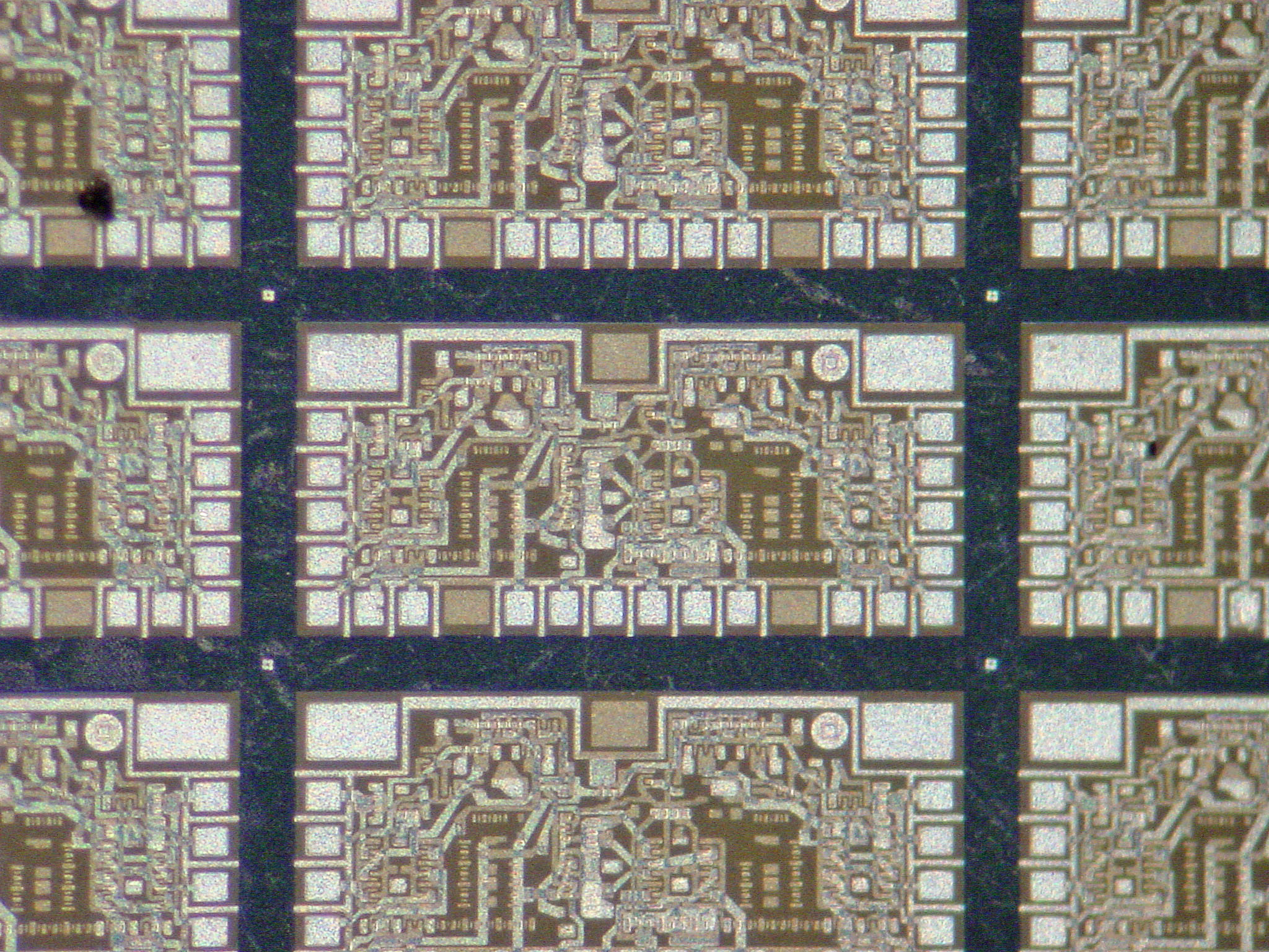
I don't know how the die size of approximately 44 mills was chosen. The die package had a 51.5 mil square cavity, so the maximum die size was set and frozen very early. This die had 44 wire bonding pads in a single rank: around the perimeter and three levels of metal. 12 pads on a side was very tight, but wire bonding at this density was never an issue in prototype production.
Layouts originally had no guidelines for the phenomena of aluminum migration by high currents. When the phenomena surfaced on the model 95, we checked our layouts. We found that we had created current densities of up to 1 million amps/square cm, and the new guideline was 100,000. In spite of the shock of finding this large problem late in a development cycle, we in fact were able to change the layouts to the new guideline without materially affecting the layout density.
The die was laid out as a tightly packed custom circuit layout, with three layers of metal. Layouts achieved densities of 40 circuits per die. The use of metal options on one diffusion was utilized. A small die, with 22 I/Os on approximately 20 x 40 mils was also designed for "unit logic" applications. Two of these small die were used in a single package.
Cesare Galtieri created a simulator of the Motorola production line. We exercised this with Motorola's projected yields and our projected change rates in development. The conclusion was that over the development cycle we would get some full custom parts back in a week, and some other parts would be so delayed by bombed lots and our own EC rate that it would not emerge until 9 months had passed. We believed we could manage this scheduling problem with the aid of premade unit logic chips and wire changes. At ACS we never had the opportunity to verify if this was so. (Interestingly enough while at Amdahl in 1972 we ran a gate array chip design but essentially the same Motorola ECL process on the same line. Over ~ 150 chip releases, the fastest turn around time for the customized two layer metal process without special incentives was 4 days. The slowest, after 3 rounds of EC's which required restarts, took 9 months. Cesare got it right!)
Circuit Speed: With a fan in of 3 and a fan out of 3, but essentially no wire, a circuit delivered under 1 ns worst-case delay.
Signal Wires: "Long" wires were terminated (at the far end) 50 ohm coaxial transmission lines, using a solid low dielectric insulation, and a plated outer shield which was grounded, yielding an overall propagation velocity of 8~9 inches per ns. Outside diameter was 10 mils. A wire preparation station was built, which would cut this coax to a specified length, attach a pig tail to the shield, and preform the coax into a staple shape with two 1 mil wires protruding at each end (the inner wire and the shield connection). A wiring station would then bond these ends to the package. The stiffness of these 1 mil wires would ultimately lead to this coax approach being replaced by twisted pair.
"Short" wires were single conductors, with a maximum length up to half the expected rise time of the signals; thus less than 0.5 ns long or about 4 inches total for the length of a net. To the degree that printed wires could be used, the increased dielectric constant of epoxy glass insulators limited nets to under 2 inches. This view led package development toward dependency on discrete wires, and viewed printed wires as nearly useless.
Chip Package: The chip package had several goals. (1) The package had to be robust to hermetically seal the chip against the known problems of moisture and the unknown problems of immersion in an initially unspecified cooling fluid. Coolant cavitation was a physical abrasion problem, which also concerned us. (2) Signals and power had to connect the chip though low resistance and inductance for speed and noise control. (3) The thermal capability had to transfer up to 3.5 watts from the chip to a liquid coolant with minimal temperature rise. The actual electrical and thermal design parameters were slightly modified as the design evolved, but min max junction temperatures stayed in the range of 15 C (essentially no power start up mode) to 45 C (with a hot chip in a hot coolant).
Second Level Packaging: The second level package was a 1.0 in2 PB board mounted in a 256 pin lead frame. There were 25 of the 44 lead chip packages mounted on the PC board in a 5 x 5 array. Planes in the PC board were used for power distribution and discrete wire was bonded on the backside of the PC board for all interconnects. The PC board was then wire bonded to the lead frame.
A silicon chip with 40 transmission line terminating resistors was also fabricated by Motorola and packaged in the same 44 lead chip package used for the circuits. These terminator chips were part of the 25 chips mounted on the second level package.
With 25 chips each dissipating up to 4 Watts each, the total power dissipation for the second level package was close to 100 Watts.
Cooling Technique: Immersion cooling was selected, using a Freon-like Coolant. This coolant cost twice the price per quart of good scotch! Pot-boiling was considered, but temperature control targets lead us to a forced convection system. The design had no problem dealing with 0 to 50 w per cubic inch power densities delivered to the coolant, while maintaining junction temperatures under 45C. (Note for perspective that 50 w/cu in is also the power density of the heating element in your clothes dryer. By contrast, air cooled equipment at that time typically lived with a power density of 1 w /cu in.) The heat exchanger/pumping station for the coolant was a frame roughly 6 ft high and 8 ft long.
All in all, this was a system with unexplored safety and reliability issues, but it worked superbly to maintain temperature control in a very hot environment with dynamic heat loading.
Test Technology: At the beginning of the ACS Project, testing of semiconductors was done, at least in IBM, with the use of custom equipment consisting primarily of analog circuits. Bill Mooney had worked in San Jose before joining ACS and was very familiar with the Model 1800 process control computer that IBM was currently shipping. He suggested that it had all of the ACS used the then new IBM 1800 process control computer as a test station. It worked superbly. Wafer probing was done at low repetition rates so power was not a major problem. Packaged chips needed to be tested at high power, so a test station was constructed with a small vertical spout of Freon. The cooling stud of the chip package dropped into the fountain, and electrical contacts were made in air above the fountain. Thermal integrity and electrical integrity was excellent.
Propagation Delay testing was also done using the 1800 computer digital and analog interfaces to drive commercially available pulse generators and a Tektronix sampling oscilloscope. We were able to find inexpensive "Crystal-Can" relays that turned out to be very close to a 50 ohm transmission line. One relay tree was used to deliver a pulse to the chip and a second relay tree was used to measure the output pulse. The path through these relay trees could propagate a pulse with a rise time significantly faster than one nanosecond. The delay tester was software calibrated for all paths so exact tuning of all the coaxial cables was not necessary. Delay test results had a repeatability of less than 50ps.
This whole approach of using general-purpose digital computers as the core of test equipment worked very well, but was not adopted by other teams in IBM until ASC was terminated and the ACS equipment distributed to other divisions. By a year or two later, the approach was standard in IBM.
Design Tools: The computers used by the ACS team were a 360/75 as the computer room mainframe, and scattered 1800's and 1620's for dedicated functions. Time on the mainframe was as is always the case with mainframes, hard to get.
Most circuit analysis was done on the 1620. A first generation Spice Model was constructed and Fortran was used to a DC Simulator and a Time Domain Simulator similar to what Berkeley later created as SPICE. It included all known effects - circuit parameters, temperature, package thermal characteristics, power distribution, plating resistance, transition line parameters, etc, etc. Delay and noise margin was predicted. As we learned details about one component, and lost margin, we would change the manufacturing specification of other parts or make a change to an adjustable parameter. The process worked very well, and allowed easy trade-offs between specifications that normally involve cross department or cross company negotiations.
Chip layout was done by hand, with the aid of a graphics checking program that ran on the model 75. Output was to a plotter that would cut rubylith at 1000x actual size This was a long, slow process, but first samples were made that were fully functional and met speed requirements. We also processed 13 EC's on the first two die, not logic but all circuit and process margin issues, and all with the work in process guideline of "use as is, don't scrap". That was a measure of how fast we were moving in uncharted waters, with our heads just above water.
The circuit/silicon goals of speed, density, cost, and production capability were met. Circuit instability was never observed. Circuit speed of 1 ns for a loaded circuit with 50 ohm drive was achieved with solid margins. When the ACS program ended, control of this silicon technology was transferred to the Components Division. By then they believed that they had a similar capability in-house, and terminated the Motorola contract. IBM then offered essentially the same silicon technology in-house, and Motorola offered it as a commercial supplier.
The package technology had the goal of 10x wire length reduction over what was available at the start of the program such as the still in development 360/95. The ACS technology offered the following:
| Item | Effect on Wire Delay (vs 360/95 like package) |
|---|---|
| 40 gates per chip (60 output nets), partitioned typically to 2/3 internal to chip, 1/3 external. Thus 2/3 wires reduced to ~ 0 |
3 x improvement |
| Point to Point Wire | Average 1.2 x improvement, but the worst wires get the biggest improvement. |
| Wire dielectric - Air & Teflon | 2 x improvement |
| Miniature package dimensions | 2 x improvement |
| Lots of custom circuits (chips) fewer I/O pins used than with more standard partitioning of logic. |
~ 1.5 x improvement |
| Overall Effect | 22 x potential improvement, toward a 10 x goal |
It seems reasonable to conclude that the ACS system had an excellent prospect of reaching its' performance goals of a 10 ns cycle.
This technology was not adopted by anyone when the project was terminated. Big mainframes did not reach a 25 ns cycle until approximately 10 years later; and microprocessor designs achieved 10 ns approximately 20 years later.
This was likely a missed opportunity to produce a high performance computer that was considerably faster than the competitive standards for one to two decades.
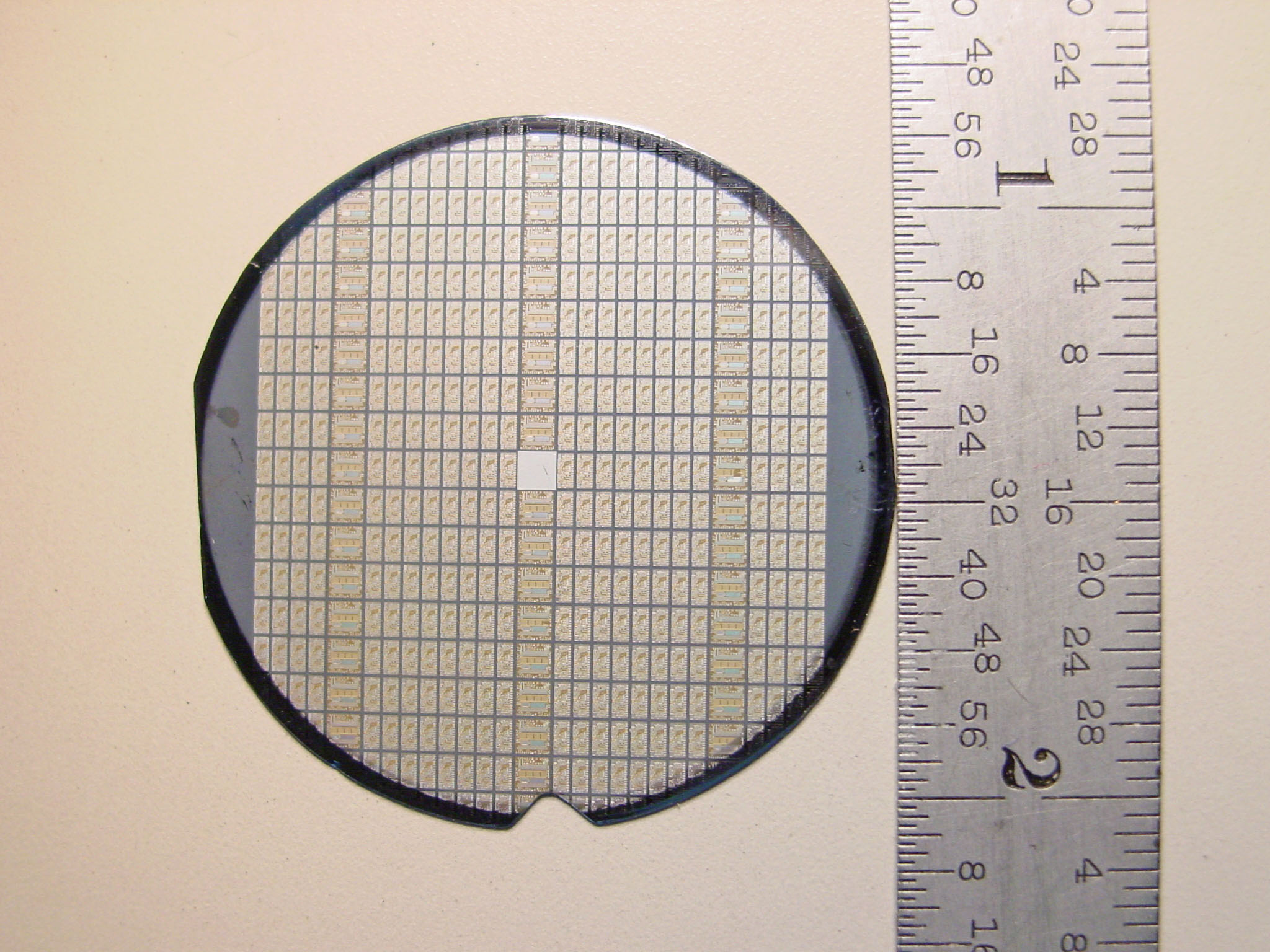
Photos courtesy of John Zasio. Top photo is an ACS wafer with the half-size die, and bottom photo is a close up of the half-size die. The half-size die has five circuits.